![[Home]](http://www.bayleshanks.com/cartoonbayle.png)
---
Freedom U500, Linux-capable, 1.5GH quad-core RV64GC SoC?: Jack Kang
    Freedom Unleashed 500: 250M+ transistors, TSMC 28nm, high-performance integrated RISC-V SoC, U54MC RISC-V CPU Core Complex
    1.5GHz+ SiFive E51/U53 CPU. 1xE51 (16KB L1I$, 8KB DTIM), 4 x U54. 32KB L1I$, 32KB L1D$.
---
Celerity: An Open Source 511-core RISC-V Tiered Accelerator Fabric: Michael Taylor
511 RISC-V cores •5 Linux-capable RV64G Berkeley Rocket cores •496-coreRV32IMmesh tiled array “manycore” •10-core RV32IM mesh tiled array (low voltage)
The BaseJump? manycore architecture implements the RV32IM with a 5-stage pipeline (full forwarded, in-order, single issue). It has 4KB+4KB instruction and data scratchpads.
5 Berkeley Rocket Cores(https://github.com/freechipsproject/rocket-chip) •Generated from Chisel •RV64G ISA •5-stage, in-order, scalar processor •Double-precision floating point •I-Cache: 16KB 4-way assoc. •D-Cache: 16KB 4-way assoc
The tiled architecture 496 RISC-V Cores Scratchpad memory: 4KB for I Mem, 4KB for D Mem
Configuration Normalized Area (32nm)
Celerity Tile@16nm D-MEM = 4KB I-MEM = 4KB
OpenPiton? Tile@32nm L1 D-Cache = 8KB L1 I-Cache = 16KB L1.5/L2 Cache = 72KB 1.17 mm2
Raw Tile@180nm L1 D-Cache = 32KB L1 I-SRAM = 96KB
MIAOW GPU Compute Unit Lane @32nm VRF = 256KB SRF = 2KB
---
Binarized Neural Networks •Training usually uses floating point, while inference usually uses lower precision weights and activations (often 8-bit or lower) to reduce implementation complexity •Rastergariet al. [3] and Courbariauxet al. [4] have recently shown single-bit precision weights and activations can achieve an accuracy of 89.8% on CIFAR-10
---
the tiny KickSat? satellite project used MSP430s on its Sprite nanosatellites. The use Energia, a port of Arduino to MSP430s, to program it.
Aaccording to [1] and [2], the MSP430 used is:
It has 32KB Flash and 4KB RAM (both the specs and also KickSat?_SmallSat?.pdf give these numbers of flash and RAM).
" The CC430 SoC? is the core of the Sprite, providing all computing and communication capabilities. It combines an MSP430 microcontroller,which is clocked at 8 Mhz and provides 4 kB of RAM and 32 kB of flash memory, with a very flexible CC1101 UHF transceiver capable of output powers up to 10 mWand data rates up to 500 kbps. Both the MSP430 and CC1101 have flight heritage on CubeSat? missions."
---
" (From the Erlang website (http://erlang.org/faq/implementations.html): "Getting Erlang to run on, say, an 8 bit CPU with 32kByte of RAM is not feasible. People successfully run the Ericsson implementation of Erlang on systems with as little as 16MByte of RAM. It is reasonably straightforward to fit Erlang itself into 2MByte of persistant storage (e.g. a flash disk).") "
---
initial AVR device, AT90S8414, noted in The AVR Microcontroller and C Compiler Co-Design:
---
S Gupta et al , Deep learning with limited numerical precision, icml 2015, shows that 14-bit 'floats' are enough for deep learning (i think; i just saw one slide in a sorta-related talk)
---
currently can simulate a 56-qubit system with a large classical computer. Expect that this ability to simulate quantum computers will max out at somewhere between 50 and 100 qubits. [3]
currently 20- and 50- qubit machines are available [4]
" Universal fault-tolerant quantum computers will require error-free execution of long sequences of quantum gate operations, which is expected to involve millions of physical qubits. Before the full power of such machines will be available, near-term quantum devices will provide several hundred qubits and limited error correction. "
---
Google Tensor Processing Unit 2 uses 32-bit math but also says "MXU: 32b float accumulation but reduced precision for multipliers"
http://learningsys.org/nips17/assets/slides/dean-nips17.pdf
" Some Example Questions Precision : Will very-low precision training (1-4 bit weights, 1-4 bit activations) work in general across all problems we care about? "
" Reduced precision benefits inference (memory bandwith 8Bit=Factor 4). Weights in layers are Gaussian. Store Min & Max in each layer and quantize numbers to closest 8Bit. Quantization is treated by model like noise. If susceptible to noise: bad model due to lack of generalization.
Probably training suffers (lower partial derivatives precision means slower convergence due to larger iteration number), plus vanishing gradient problem.
Training demands increase with number of trainers/researchers. Inference demands increase with number of users; plus RealTime? requirements.
Conclusion: Reduced precision or quantization may be more important than parallelization. ... Quantization is hot and (very recently) even binarization. ... 65k 8Bit int multipliers (compare GPU: <<10k 32Bit Floatingpoint multipliers) ... Idea: * from Multiply/Accumulate/NonLinFunction? with 32/16Bit Floatingpoint to reduced accuracy by 8Bit quantization 4 IntegerOps? Result: 1/4 memory 4 model " [5]
" For example, neural nets can be compressed by using 4- or 8-bit integers instead of 32- or 64-bit floating point values to represent the model parameters (a process referred to as quantization). "
---
note: this link is notes that list a lot of interesting 'deep learning coprocessing' machines and similar (putting in square brackets because i'm not really interested in such a list at this moment):
this link has another such list:
---
"Usually the ((user)) stack size is unlimited", no, usually it limited by 8Mb (ulimit -s). – Eddy_Em Feb 5 '13 at 6:57
"The kernel stack is fixed always (usually 8KB)" [7]
---
not 'low end' but..
https://www.electronicsweekly.com/news/design/xilinx-wins-space-design-2017-01/
"FPGAs are at the heart of processing in Iridium NEXT satellites launched a few days ago, according to Xilinx. ... Virtex-5QVs are built on the second-generation ASMBL column-based architecture of the Virtex-5 family with support in Xilinx’s ISE Design Suite.
They include hard IP for 36kbit/18kbit block RAM/FIFOs, second generation 25×18 DSP slices, 18 channels of 4.25Gbit/s transceivers and PCI Express-compliant endpoint blocks.
On die are 130,000 logic cells, 320 DSP Slices (fixed and floating point) and 836 user I/Os (programmable to >30 standards). "
iridium next also has a LEON3 processor. not sure if it's this one:
"
LEON3FT SPARC V8 32-bit Processor ... 1.4 DMIPS/MHz – Multi-processor support (AMP/SMP) – •Cache size 1 – 256 KiB?, 1-4 ways •Hardware Mul/Div/MAC options •MemoryManagamentUnit •Floating-pointunit –Detect and correct SEU in all on-chip RAM memories
and the old/current iridium constellation:
" The satellites each contain seven Motorola/Freescale PowerPC? 603E processors running at roughly 200 MHz,[6] connected by a custom backplane network. One processor is dedicated to each cross-link antenna ("HVARC"), and two processors ("SVARC"s) are dedicated to satellite control, one being a spare. Late in the project an extra processor ("SAC") was added to perform resource management and phone call processing. "
" 32-bit PowerPC? Architecture ... The performance issues of the 603 were addressed in the PowerPC? 603e. The L1 cache was enlarged and enhanced to 16 kB four-way set-associative data and instruction caches. .. The PowerPC? 603e was the first mainstream desktop processor to reach 300 MHz, as used in the Power Macintosh 6500...The PowerPC? 603e was also the heart of the BeBox? from Be Inc. The BeBox? is notable since it is a multiprocessing system, something the 603 wasn't designed for. IBM also used PowerPC? 603e processors in the ThinkPad? 800 series laptop computers...The 603e processors also power all 66 satellites in the Iridium satellite phone fleet. The satellites each contain seven Motorola/Freescale PowerPC? 603e processors running at roughly 200 MHz each "
---
according to [8], "Intel introduced the first commercial microprocessor, the 4-bit Intel 4004, in 1971"
the https://en.wikipedia.org/wiki/Intel_4004 had
"
    12-bit addresses
    8-bit instructions
4-bit data wordsso:
---
" I’m amazed that if your budget for a board was just $5 for one MCU board, you now have so many options for your electronics projects: ESP8266 boards, a few STM8 boards, One Dollar Board project, and many more… Other options are “BluePill” or “RedPill” boards based on STM32 or GD32 32-bit ARM Cortex M3 micro-controllers that go for about $2 shipped, and can be programmed with the Arduino IDE thanks to STM32Duino project. "
" BluePill? board specifications:
MCU – STMicro STM32F103C8T6 ARM Cortex-M3 MCU @ 72 MHz with 64KB flash memory, 20KB SRAM."
so yeah, my "32k ROM 4k RAM" target for language stuff still sounds good here; that consumes half the ROM and 20% of the RAM of this system, leaving the rest for the application. In fact this suggests that we might be able to stand 8k RAM usage.
Also interesting that ARM Cortex M3, not M0 or M1, are so common/cheap -- this suggests that we might be able to target M3 instead of M0.
---
The NVIDIA Tegra X1 CPU architecture has four high performance ARM Cortex A57 cores. The Cortex A57 CPU complex on Tegra X1 shares a common 2MB L2 cache, and each of the four CPU cores has a 48KB L1 instruction cache and a 32KB L1 data cache
(this is used in the Nintendo Switch)
---
stuff mentioned on
micro:bit adafruit circuit playground express minecraft chibi chip seeed grove zero sparkfun inventors kit wonder workshop cue
micro:bit (this is just the main CPU, there is also a secondary MCU for USB and voltage reg): "Nordic nRF51822 – 16 MHz 32-bit ARM Cortex-M0 microcontroller, 256 KB flash memory, 16 KB static ram, 2.4 GHz Bluetooth low energy wireless networking. The ARM core has the capability to switch between 16 MHz or 32.768 kHz.". Supports MicroPython?. $17
adafruit circuit playground express "". Supports CircuitPython?, a MicroPython? derivative. ATSAMD21 ARM Cortex M0 Processor, running at 3.3V and 48MHz. "The ATSAMD21G18 has 32K of RAM" [9]. Plus 2 MB of SPI Flash storage. "there's a limited amount of RAM, we've found you can have about 250-ish lines of python (that's with various libraries) before you hit MemoryErrors?". "Integers can only be up to 31 bits. Integers of unlimited size are not supported.". $25
chibi chip: Can't find specs on the underlying MCU. $30
seeed grove zero: Can't find specs on the underlying MCU(s). $100
sparkfun inventors kit 4.0: has a sparkfun "redboard", which has a . ATmega328. According to https://www.sparkfun.com/standard_arduino_comparison_guide , the Redboard has a ATmega328P with 2KB RAM and 32KB flash. $100 for the inventors kit, but the Redboard is $20.
wonder workshop cue: this is a semi-programmable robot. i can't find specs with RAM. $200
So, it sounds like a target of 32k ROM/4k RAM would be good, and my current target of 32k 16-bit words (so 64kB) ROM and 4k 16-bit words (so 8kB) is still reasonable.
---
the commodore 64 had 64k but most of that was mmapped ROM?:
"64 KB, of which 38 KB (minus 1 byte) were available for BASIC programs
...
Memory map Address Size [KB] Description 0x0000 32.0 RAM [102] 0x8000 8.0 RAM Cartridge ROM [102] 0xA000 8.0 RAM Basic ROM [102] 0xC000 4.0 RAM [102] 0xD000 4.0 RAM I/O Character ROM [102] 0xE000 8.0 RAM KERNAL ROM [102] " -- [10]
but i think that just means the RAM was banked, because also elsewhere you see
" the Commodore 64 came with 64K of RAM, and had 20K of ROM, running a 6510 microprocessor (a modification of the 6502). It accomplished its RAM and ROM combination through bank switching, much as the Apple II did with its 16K language card. " [11]
this dude connected an ipod nano to an old apple ii. of interest is this part that says that the ipod nano's screen takes 8k memory locations to store, and the apple ii's takes 10k: "Since the iPod Nano screen is pretty low-res to begin with I just map each pixel into an 8k framebuffer, then transfer it directly into the Apple Hi-Res screen, with 2Kbytes to spare!" [12]
---
alyandon 13 hours ago [-]
Showing my age a bit but it's amazing how such simple things can alter one's life. My parents brought home a heavily discounted TRS-80 Model I Level I with a whopping 4k of ram when I was a child and that started my life long love of technology/coding.
reply
cr0sh 12 hours ago [-]
I started programming in Microsoft BASIC on my first computer - a TRS-80 Color Computer 2 with 16K of RAM. I used a cassette tape drive for storage, and a television for my "monitor".
That's where it all began. Upgrades were done (went to 64K of RAM, also got a floppy drive and printer - then later the Color Computer 3, which was upgraded to 512K, and the CM-8 monitor - oh, there was a 300 baud modem in there somewhere too).
---
" Mostek MK4096 4-Kilobit DRAM (1973)
Mostek wasn’t the first to put out a DRAM. Intel was. But Mostek’s 4-kilobit DRAM chip brought about a key innovation, a circuitry trick called address multiplexing, concocted by Mostek cofounder Bob Proebsting. Basically, the chip used the same pins to access the memory’s rows and columns by multiplexing the addressing signals. As a result, the chip wouldn’t require more pins as memory density increased and could be made for less money. There was just a little compatibility problem. The 4096 used 16 pins, whereas the memories made by Texas Instruments, Intel, and Motorola had 22 pins. What followed was one of the most epic face-offs in DRAM history. With Mostek betting its future on the chip, its executives set out to proselytize customers, partners, the press, and even its staff. Fred K. Beckhusen, who as a recent hire was drafted to test the 4096 devices, recalls when Proebsting and chief executive L.J. Sevin came to his night shift to give a seminar—at 2 a.m. “They boldly predicted that in six months no one would hear or care about 22-pin DRAM,” Beckhusen says. They were right. The 4096 and its successors became the dominant DRAM for years. " [13]
" He didn’t, of course. In 1984 he presented a paper on his memory design at the IEEE International Electron Devices Meeting, in San Francisco. That prompted Intel to begin development of a type of flash memory based on NOR logic gates. In 1988, the company introduced a 256-kilobit chip that found use in vehicles, computers, and other mass-market items, creating a nice new business for Intel. " [14]
" The Ferranti Mark 1’s unique memory system (part of which is shown above) could store just over a kilobyte of data in cathode-ray tubes for high-speed access; a rotating magnetic drum offered 82 kilobytes of permanent storage. " [15]
---
https://en.m.wikipedia.org/wiki/Atari_Jaguar
"Graphics processing unit (GPU) – 32-bit RISC architecture, 4 KB internal cache, all graphics effects are software based.
...
Digital Signal Processor – 32-bit RISC architecture, 8 KB internal cache
...
RAM: 2 MB on a 64-bit bus using 4 16-bit fast page mode DRAMs (80 ns)[37] Storage: ROM cartridges – up to 6 MB
Motorola 68000 "
---

The 8080A had 78 instructions, 7 addr modes, 8 registers. The Z80 had all of the 8080A instructions and more, for a total of 158, and 11 addr modes and 17 registers. The Z80 development system had 16k memory, expandable to 60k, plus 4k bytes of "RAM/ROM monitor software".
---
In https://en.wikipedia.org/wiki/Stochastic_computing , a candidate neural code, you need 2^n the usual number of bits; so O(256) bits to represent an 8-bit number, O(64k) bits to represent a 16-bit number, etc. If neuronal refractory periods are around 2ms, and response times are about 500ms, then we certainly don't have room for more than 250 bits transmitted in serial (however, this probably doesn't mean anything because the needed number of bits could be, and probably are, transmitted in parallel rather than in serial).
---
"Osborne’s VLIW processor design required a 64-bit-wide read-only memory (ROM). Although the HP 9100A’s processor was actually a microprogrammed state machine and didn’t run software in the conventional sense, state-machine design can employ a control ROM to direct the machine’s operations during each state, to test branch conditions, and to specify a next state. Osborne determined that the HP 9100A would, at a minimum, need a 32-kbit ROM, organized as 512 64-bit words. The HP 9100A could have used more ROM capacity, but even 32 kbits was well beyond the state of the art for 1965-era electronics. In fact, it was completely beyond the reach of the integrated-circuit technology in 1965, which was barely able to pattern 50 devices (transistors, diodes, and resistors) on one chip; forget about 32,768 bits of IC memory.
...
The 32-kbit pc-board ROM was not the only ROM used in the HP 9100A. The HP 9100A processor design employed 29-bit microcode instructions but it had only 64 different instructions. Sixty four instructions can be encoded in only 6 bits (although sparse instruction-word coding is quite typical of a microcoded state-machine design because it saves decoding circuitry). To save bits in the HP 9100’s pc-board ROM, each of the 64 microcoded instruction words is represented by a value in a 6-bit field within the pc-board ROM’s 64-bit microcode word. This approach saved 23 bits per instruction word and kept the problematic circuit-board ROM’s word size to a barely manageable 64 bits. However, as a result of this bit compression, the HP 9100A needed additional circuitry to expand the microcode instruction field from 6 bits to 29. Today, we’d use a simple semiconductor ROM or a programmable-logic device to perform this expansion, but such technology was far beyond reach in 1965.
...
three primary registers (X, Y, and Z) and sixteen additional registers (labeled in hexadecimal as “0” through “9” and “a” through “f”). ...
Each register in the HP 9100A could hold one floating-point value (a 10-digit, signed mantissa and a 2-digit, signed exponent). Registers “0” through “9” and “a” through “d” could also hold 14 program steps each, for a total capacity of 196 program steps. (HP 9100A programming enthusiasts would quickly bump up against the calculator’s programming capacity and HP would scramble to offer more memory in the updated version of the calculator, the HP 9100B.)
...
An HP 9100A program step was synonymous with a keycode and the calculator had 62 keys, so each keycode required 6 bits of storage. Each calculator register could thus hold either 16 numerals or program steps, however the actual capacity as implemented in the HP 9100A was 14 BCD digits (to make one floating-point number) or 14 program steps per register. (Note: although a 6-bit-wide memory may seem quaint today, it was a standard word width in the early 1960s. For example, IBM’s early mainframe computers used 6-bit words until its System/360 shipped in 1965.)
...
Alternatively, auxiliary registers 0 through 9 and a through d could store 14 program steps each, for a total of 192 program steps. Registers X, Y, Z, e, and f could only hold floating-point numbers, not program steps. With registers X, Y, and Z added to the 16 auxiliary registers, the HP 9100A had 19 user-accessible registers but the HP 9100A’s core memory implements 23 registers. The remaining four registers were not user-accessible and were used for internal storage of intermediate values and machine state. Osborne also used the extra register bits and the extra 6-bit words scattered throughout the precious core memory to encode other information needed to control and operate the calculator.
...
((see pictures next to section 'Physically mapped programming, a key per function' for the available instructions))
...
The HP 9100’s Z register provides temporary, visible storage for more complex calculations. The X, Y, and Z registers constitute the RPN register “stack.” When HP developed other generations of RPN calculators such as the HP 35, it added a fourth register called the T register for additional temporary storage. However the HP 9100A had only a 3-register stack. " -- [16]
" Stack manipulation keys included an enter key (labeled only with an upward arrow), a drop key (labeled with a downward arrow) as well as ROLL keys for both directions and an X and Y exchange key. (X<->Y.)
There were 16 storage registers (32 on the HP-9100B) labeled 0-9 and a-f. There were also keys to store X or Y. Pressing a-f alone recalled that register into X and there was a key to exchange Y with any register. The HP-9100B had two pages of core with the registers 0-9 and a-f on each page. The pages were labeled + and - and + was assumed if neither was specified for a store or recall.
...
((see picture of keyboard 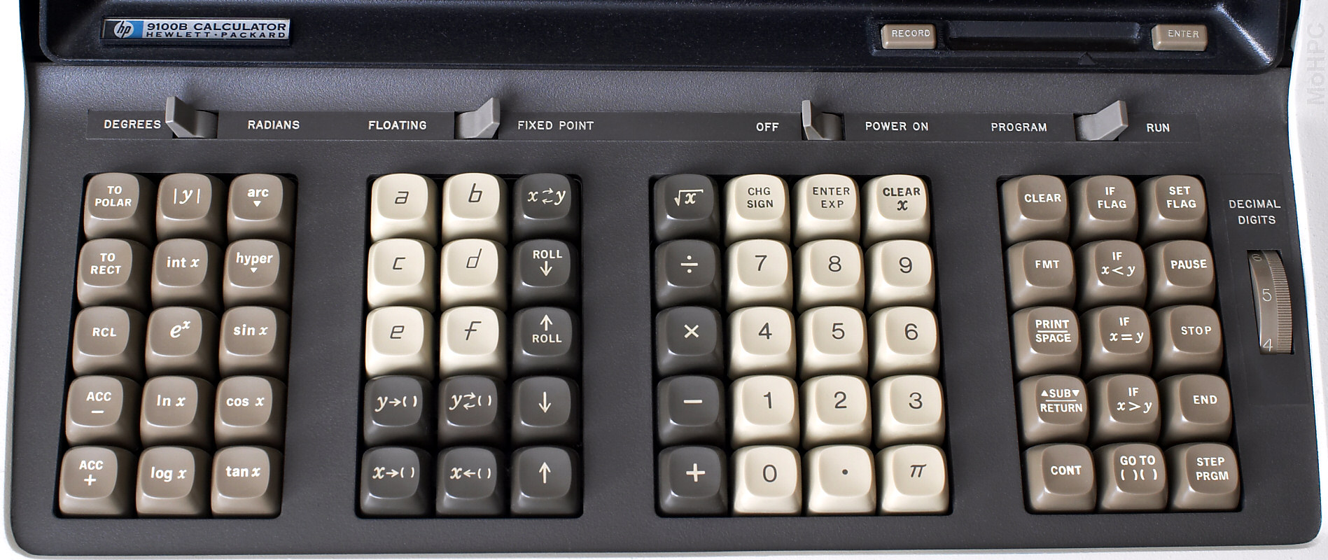 ) " -- [17]
" The program ROM contains 512 64-bit words. " -- [18]
" Magnetic core memory contains 19 registers: 3 displays registers (keyboard, accumulator, temporary) and 16 storage registers, with store/retrieve controls. These registers may be used to store 16 constants, or 196 program steps plus 2 constants, or a combination of constants and program steps. The read-only memory contains over 32,000 bits of fixed information for keyboard routines. ...
It is interesting to note that computer performance of this size was state-of-the-art just one year before the first moon landing.
Price: $4900. (Average cost of a new car in the USA in 1968 was $2800)
...
The HP 9100A was introduced first in 1968 with maximums of 16 storage registers and 196 program steps.
The HP 9100B, in 1970 doubles this capacity with maximums of 32 storage registers and 392 program steps. On both machines, core was shared between registers and program steps. (The 9100B had two pages of core.) The HP 9100B also added subroutines, a dual program display, and a key to recall numbered registers into X.
The HP 9101A Extended Memory, was introduced in the 1971 catalog supplement. It is a rack mountable box of core memory providing an additional 3472 program steps or 248 data registers. This option could be added to either model.
...
Three Models, HP 9800 10 / 20 / 30, ... ROM size: ((4k to 31k)) ... RWM size: ((128 to 7616)) ...
The 9845A had four I/O slots in which could accept the same interfaces as the HP 9825. The 9845A was shipped with 13K RAM standard, expandable to 62K. A "B" version replaced the 9845A in 1979. The original 9845B came standard with 56K RAM, expandable to 449K.
...
" -- [19]
" The HP 9100 contained 32K bits (512 64 bit words) of ROM program memory
" -- [20]
programming details: https://www.scss.tcd.ie/SCSSTreasuresCatalog/hardware/TCD-SCSS-T.20121208.016/HPmuseum.org-HP9100A-Programming.pdf
---
"During this period, the computer market was moving from computer word lengths based on units of 6-bits to units of 8-bits, following the introduction of the 7-bit ASCII standard." [21]
---
" Unibus models
The following models use the Unibus as their principal bus:
PDP-11/20 and PDP-11/15 — The original, non-microprogrammed processor; designed by Jim O'Loughlin. Floating point is supported by peripheral options using various data formats. The 11/20 lacks any kind of memory protection hardware unless retrofitted with a KS-11 memory mapping add-on.[14] PDP-11/45, PDP-11/50, and PDP-11/55 – A much faster microprogrammed processor that can use up to 256 kB of semiconductor memory instead of or in addition to core memory; support memory mapping and protection.[14] First model to support an optional FP11 floating-point coprocessor, which established the format used in later models. "
" The PDP-11/20 was the first PDP-11 ...
The -11/20 did not have, as standard components, many of the capabilities that later became standard on later models, such as hardware multiply and divide, floating point, and memory mapping. DEC provided a series of accessories that provided some of these capabilities.
One was a co-processor for the multiply/divide instructions; rather than additional instructions in the CPU, it was implemented as a device on the bus, making this model incompatible from the rest of the PDP-11's.
...
hampage.hu Quoted... The PDP-11/20 is a general-purpose computer with a wordlength of 16 bits. It features 8 general registers, and one interconnect for all system components (CPU, memory, peripheral devices), the UNIBUS (which is not the successor of the PDP8 OMNIBUS). This bus had an addressing range of 18 bits, but only 16 were used, which led to the 32 Kword (as mentioned, one word was 16 bits, so this is equal 64 Kbyte) memory limit. As with the other members of the -11 family, the top 4 KW of the memory is reserved to the system (the upper memory addresses refer to devices connected to the CPU). It is also interesting to know that most machines were shipped with only 12 KW of magnetic core memory. "
so.. even the first PDP-11 had 24k bytes of memory, usually; but not all of them did:
" PDP11/15 A strip down of the PDP11/20, with 2Kb of read-only memory (rope core) and 256 bytes of read/write memory. "
"
PDP11/20 This is the first model of the series, and the only one to be hard wired instead of using microcode for the instruction decoding. The base model had 8Kb of core memory, an ASR-33 teletype (with reader and punch) and was available in a table top or rack mount box. " [24]
" PDP-11 M9312
As this PDP-11 website explains:
The M9312 Bootstrap/terminator module contains a complete set of UNIBUS termination resistors and 512 words of ROM that can be used for diagnostic routines, the console emulation routine and bootstrap programs. The module has 12 jumpers, W1 thu W12, and five sockets to put ROMs in. One socket is used for a diagnostic ROM for the PDP-11/60 or PDP-11/70, or for a ROM that contains the console emulation routine and diagnostics for all other PDP-11s. The other four sockets accept ROMs that contain bootstrap programs.
"
---
the original SpaceWar? game on the PDP-11 was about 4k [26] a little after minute 13.
You can see the 12k of memory in the machine at 19:06.
---
Const-me 1 day ago [-]
> the handwritten text is not always clear and could reasonably be interpreted differently
Digital pen input contains more info than the resulting bitmap; strokes are lost while rasterizing.
That info was the reason how old devices were able to reliably recognize characters written by a stylus. It worked well even on prehistoric hardware, such as 16MHz CPU + 128 kB RAM in the first Palm PDA.
---
IBM is said to be making a 1mm^2 computer, smaller than the Michigan Micro Mote (see above), previously the smallest. But they don't provide specs yet:
---
"The arduino only has 2K of RAM ... Two that I am interested in are:
teensy - $20 - 64K of RAM, 72MHz Cortex-M4. Can use many Arduino libraries.
Raspberry Pi - $25-35, 512MB of RAM, 700MHz ARM1176JZF-S." [27]
---
"gokrazy is a pure-Go userland for your Raspberry Pi 3 appliances
For a long time, we were unhappy with having to care about security issues and Linux distribution maintenance on our various Raspberry Pis.
...
Your app(s) + only 4 moving parts
    the Linux kernel
    the Raspberry Pi firmware files
    the Go compiler and standard library
    the gokrazy userland
All are updated using the same command. "
mb see also https://github.com/u-root/u-root
---
a discussion of some other things like the PICO-8:
https://news.ycombinator.com/item?id=16967664
---
The most visible technical feature of the Pico is the 128 × 128 pixel screen with a fixed 16-colour palette. The palette has a fairly personal and easily identifiable choice of colours, and its designer has clearly had more of an eye for colour than the average engineer.
Although Pico games typically use background maps consisting of 8 × 8 pixel blocks, and 8 × 8 pixel sprites on top of them, this is not a limitation. The graphics mode is a pure pixel buffer that can be used to draw anything – and the machine is also fast enough to run 1990s demo effects smoothly. However, the platform encourages the use of 8 × 8 pixel blocks by offering functions for drawing maps and sprites that are faster than using your own code to do the same pixel by pixel.
The cart can hold 15,360 bytes of compressed code. The maximum length in the editor is 65,536 characters or 8,192 tokens in tokenised form. These limits are not easily met – even many of the best games are clearly below these figures.
The cart has 12,544 bytes reserved for graphics and 4,608 bytes for sound. Of course, these data areas can be used for other purposes – the memory handling commands allow it to be accessed at the byte level. Upon program start-up, the contents of the cartridge’s data side are copied into user RAM where the program can modify it, if necessary. User RAM also includes slightly under 7 kilobytes of space reserved for the user and 8 kilobytes of video memory.
The graphics data consists of 8 × 8 pixel sprites where the entire colour palette can be used freely. The maximum number of sprites is 256 and the map consists of 128 × 32 sprites. It is possible to double the size of the map by settling for 128 sprites.
On the sound side, the equivalent of a “sprite” is a sound effect (sfx) that consists of 32 note locations. Each note location contains the note and the waveform, volume and effect; there are 8 different types of each of these. The playback speed can be altered; lower speeds are better suited for music than sound effects.
Similarly to tracker music, a song consists of patterns that define which sound effect is played on each of the four channels. There is space for 64 patterns, which can hold several songs when loops and pattern end flags are used.
While the graphics side allows everything to be built from individual pixels, the user cannot access the “registers” of the sound system. In theory, you could build a player routine by modifying the sound data in real time, but the limits of the virtual machine’s timing might not allow this.
In addition to the program code, data RAM and cartridge ROM, the Pico offers 256 kilobytes of space for the Lua interpreter. This is a relatively large amount when compared to the Pico’s other memory spaces, but it will fill up easily with large tables, for example. One element of a number table takes up eight bytes, half of which is taken up by the actual data. Each number consists of a 16-bit integer part and a 16-bit fraction, which means that bit arithmetic operations can be used to compress them.
When running low on space, Pico can also read data from other ROM cartridges and even write to them. Program code has a strict limit, however; it can only be executed from the original cartridge. Lua in itself includes the possibility to execute data as code, but it has been removed in the Pico-8. This means that those requiring more code space will need to build their own virtual machine.
The Pico-8 does not execute Lua code as quickly as the computer’s processor allows. Execution times have been defined for the different functions. This speed limit will rarely lead to problems during the development of typical Pico software, but it standardises the limits of the platform and prevents spiralling hardware requirements. According to the authors, a first-generation Raspberry Pi is enough for running even the most demanding Pico software at full speed.
There are two functions available for drawing sprites: spr() draws an individual 8 × 8 pixel sprite at the provided coordinates, whereas sspr() draws an arbitrary area from a sprite sheet at arbitrary scaling. The scaling function enables a number of tricks that are fairly costly on most classic hardware, such as Doom-type texture mapping.
Drawing moving graphics is more reminiscent of a PC than the 8-bit home computers. The Pico has no “hardware sprites” or “hardware scrolling”. Instead, the display is usually redrawn for each refresh: clear the screen, draw the background and then draw the necessary sprites.
The sound side offers the functions sfx() and music(). The former plays the sound effect given as a parameter on the first available sound channel, the latter starts playing music from the pattern number given as a parameter.
If we had to summarise the spirit of the Pico-8 into one word, it would probably be “straightforward”. Some of this stems from the 8-bit computers and their BASIC: you can start writing your program immediately after “powering on” and never need to think about OS requirements, APIs or different execution environments. Things are simple and tangible: specific bits in a specific memory location will always mean a block of a specific colour in a specific place on the screen.
The concept goes further than that, however: there is no counting of clock cycles and raster lines, no colour cell boundaries, no juggling back and forth with utilities and files. The limits of the platform prevent arduous and time-consuming fine-tuning. Since there are no adjustable palettes, sample systems or machine code instructions, you do not need to tune them. And the small number of pixels ensures that not even a perfectionist can spend very long with the anti-aliasing.
---
hmmm the PICO-8 screen resolution is a little low for my taste, as is 16 fixed colors. Maybe the 8x8 sprites should change too, not sure. What are other 'Oregon Trail Age' computer screen sizes and palette sizes (omitting screen_size x palette limitations)?
C64 had 320x200 [29]. Note that 320*200 = 64000. C64 had 16 colors (fixed) [30]. Sprites were apparently 24x21 pixels [31].
The Apple IIgs had a 640x200 screen size and palettes of 16 12-bit colors [32]. No sprites. Looks like the Apple II font was 7x8 [33]; at 80x24 columnsXrows, that's 560x192 (matching video mode 'emulation video Double high resolution' [34], which is strictly less than 640x200.
And all these are strictly less than the modern 640x480 (VGA) [35]. The C64 screen size is on the chart [36] on that page as 'CGA', but 560x192 is larger than anything under VGA.
Note that 2^18 < 640*480 < 2^19, and 2^16 < 560*192 < 2^17.
12-bit colors can (i assume) be specified as 3 channels of 4 bits each, that is, one hex digit for each of RGB or each of HSV or something like that. If these are placed within 16-bit memory locations, then each pixel has 4 bits remaining, which could be used for alpha or similar.
I'm also curious how these things could be extended to a low-but-decent resolution 3d setup, and to vector graphics.
Perhaps a first start would be to just extend 640x480 to 640x480x480. Sprites could be extended too, but maybe watch that the voxels per sprite stays under 2^16. 32*32*32 = 215, so maybe that's the limit, if the sizing is rectangular. But we'd want some sprites to be smaller. Let's just say that sprite sizes in each dimension must be powers of 2 beween 1 and 32, inclusive. So 1,2,4,8,16,32. Unfortunately that's 3 bits per dimension, so with 3 dimensions that's 9 bits to specify a sprite size, which is inconvenient. Another thing we could do is say that the sprite sizes must be powers of 2 between 1 and 8, inclusive, in which case we have 2 bits per dimension for a total of 6 bits -- then we have 2 leftover bits per byte, so we could have a scale factor of 1,2,3,4. Alternately, we could allow sprite sizes to be any number, not just a power of 2, in each dimension, from 1 to 16 inclusive. Then that's 4 bits per sprite dimension, so 12 bits total, giving 4 bits leftover if we allocate 2 bytes of memory for sprite sizes. Alternately, we could allow sprite sizes in each dimension to be any number from 1 to 32 inclusive; then that's 5 bits per sprite dimension, or 15 bits total, with 1 bit to spare. I guess i like that the best.
Note that this could also be used for platform-supported dense array arithmetic, that is, the platform could provide special support for arrays of dimension <= 3 and size <=32 in each dimension. Recall that 32*32*32 = 215, so we're well under the 216 limit.
As for vector graphics, i don't know much about these, so the calculations will have to wait.
640x480 could fit 60 rows of 80 columns of 8x8 characters. Does this inform our terminal size? https://help.gnome.org/users/gnome-terminal/stable/app-terminal-sizes.html.en gives a choice of some standard terminal sizes; 80 columns by 24 rows, 80x43, 132x24, 132x43. So perhaps we don't want to mandate more than 43 rows. [37] says that 24 or 25 lines is pretty standard. Maybe just stick with 24 then.
80*24 = 1920, so maybe allow at least that many sprites on screen at once? Round up to 211 = 2048? Not sure about this though, because i think many systems allow much less than that and i don't really understand the technical implications.
Summary so far:
A decent set of requirements is:
---
"The current implementation is for the Mica family of nodes [5]. These nodes may be interf aced to external sensor boards and include 512K of external flash mem- ory . The y contain the Atmel ATMe ga128 microcontroller [2] with 128K program memory and 4K internal SRAM"
---
" Level I BASIC was based on Li Chen Wang’s Palo Alto Tiny BASIC. It was some of the finest assembly language code I’ve seen anywhere. Browsing through it was like an afternoon at the Louvre. " [39]
---
" Q: It was often stated that the TRS‑80 Model I was more powerful than the computer used by the Apollo lunar module. As someone who actually worked on the Apollo program, do you think that was true?
A: Yes, absolutely. I’ve heard it said that a modern digital watch is more powerful than the Apollo flight computer. When you think about it, the remarkable thing is that we had a flight computer at all. Consider: There was no such thing as RAM chips, much less CPUs. The Apollo computer used 2k of magnetic core RAM and 36k wire rope (ROM) memory. The CPU was built from ICs, but not the kind we think of today. They were, in fact, the same Fairchild RTL chips I fell in love with. Clock speed was under 100 kHz. Compare that to the 16k ROM, 16-48k RAM, and 2 MHz clock of the TRS‑80.
The fact that the MIT engineers were able to pack such good software (one of the very first applications of the Kalman filter) into such a tiny computer is truly remarkable.
Originally, NASA didn’t plan to use the Apollo computer for guidance at all. The intent was to use radio signals from the ground to control the spacecraft. We had worked up nomograms (graphs) for the astronauts to use in case they lost radio communications. Those plans got changed as the flight computer developed so nicely. " [40]
---
"
Q: Do you think the computer industry today could learn some lessons from the earlier days of computers?
A: You bet. In those days, we struggled to save bytes and clock cycles wherever we could. Today, with computer capacities and clock speeds improving by the day, I fear that too many vendors just count on the hardware to hide their inefficient code. I once read a quote from a Microsoft software manager who said, “We don’t try to optimize anymore. We just throw the software out there, and wait for the hardware to catch up.”
The thing is, even as fast as today’s computers are, the hardware really HASN’T? caught up. It still takes my PC, with a 2GHz AMD 64 x2, over a minute to boot. How many clock cycles is that? I once figured that, at this clock rate, I could have run every single FORTRAN simulation I ever wrote, 10,000 times over, just in the time this computer takes to boot. And fast as this computer compiles C code, my old Kaypro did it much faster.
Q: What’s your opinion of today’s operating systems? Is their level of complexity sustainable?
A: Funny you should ask. Just last week, I commented that I wasn’t happy with either Windows or Linux. Someone else asked, “Then what DO you like.” I didn’t have a good answer. The most recent operating system that I truly loved was CP/M. And the reasons were simple enough. First, it was small enough to understand. If there was something it was doing that I didn’t like, I wasn’t afraid to go in and replace or rewrite it. There was nothing going on in that computer, either the OS or its applications, that I didn’t understand. I don’t think, even at Microsoft, there’s anyone in the world that understands all of Windows.
Second, CP/M and its applications worked. Every time. There was no blue screen of death; no need for Disk Doctors, no forced reboots, no editors that couldn’t save their files. Someone asked me once if I’d ever had a floppy disk get corrupted under CP/M. I could honestly answer, “Only one, and that was because it had gotten so old that the oxide layer was flaking off.”
Oh, there were programs out that crashed. They got immediately relegated to the circular file. But the ones I used every day, did what I told them to do, every time, no exceptions. I miss that. If there’s anything that we’ve learned recently, about operating systems, it’s that you can only carry complexity so far. " [41]
---
" The Xbox 360 CPU is a three-core PowerPC? chip made by IBM. The three cores sit in three separate quadrants with the fourth quadrant containing a 1-MB L2 cache – you can see the different components, in the picture at right and on my CPU wafer. Each core has a 32-KB instruction cache and a 32-KB data cache. "
---
https://basicengine.org/ https://news.ycombinator.com/item?id=17674944
---
CPU MT7628AN, 580 MHz, MIPS 24K MEMORY 128MB, DDR2, 166MHz STORAGE 16M NOR on board, support SDXC up to 2TB
---
https://tomu.im/ slide 13 silicon labs happy gecko 8kb RAM 64kb flash 25Mhz ARM Cortex M0+, USB 2.0 $2.15
on the webpage (not slide): " Uses a Silicon Labs Happy Gecko EFM32HG309 25MHz ARM Cortex-M0+ 8kb^ RAM 64kb^ Flash USB 2.0 FS and LS Literally 12 parts "
slide 21 tomu has same specs (i guess it's based on happy gecko?), plus 2 buttons and 2 LEDs, $10
slide 36 $15 alternative, 48Mhz ARM Cortex M0+, 32kb RAM, 256kb flash, hardware crypto chip
EFM32HG
itomato 1 day ago [-]
They can also run Commodore 64 BASIC. Sadly, the ARM part only has 8K RAM.
https://www.pagetable.com/?p=956
reply
dtornabene 1 day ago [-]
true, but the next generation has I believe 64k (or more) of RAM.
reply
---
New RT Cores to enable real-time ray tracing of objects and environments with physically accurate shadows, reflections, refractions and global illumination. Turing Tensor Cores to accelerate deep neural network training and inference, which are critical to powering AI-enhanced rendering, products and services. New Turing Streaming Multiprocessor architecture, featuring up to 4,608 CUDA® cores, delivers up to 16 trillion floating point operations in parallel with 16 trillion integer operations per second to accelerate complex simulation of real-world physics.
First implementation of ultra-fast Samsung 16Gb GDDR6 memory to support more complex designs, massive architectural datasets, 8K movie content and more. NVIDIA NVLink® to combine two GPUs with a high-speed link to scale memory capacity up to 96GB and drive higher performance with up to 100GB/s of data transfer.
GPU Memory Memory with NVLink Ray Tracing CUDA Cores Tensor Cores Quadro RTX 8000 48GB 96GB 10 GigaRays?/sec 4,608 576 Quadro RTX 6000 24GB 48GB 10 GigaRays?/sec 4,608 576 Quadro RTX 5000 16GB 32GB 6 GigaRays?/sec 3,072 384
Quadro RTX 8000 with 48GB memory: $10,000 estimated street price
Quadro RTX 6000 with 24GB memory: $6,300 ESP
Quadro RTX 5000 with 16GB memory: $2,300 ESP
---
"An exception to the rule that GPUs require a host is the NVidia Jetson, but this is not a high-end GPU.)"
https://developer.nvidia.com/embedded-computing https://developer.nvidia.com/embedded/faq
Jetson TX2/TX2i
GPU NVIDIA Pascal, 256 NVIDIA CUDA Cores CPU HMP Dual Denver 2/2MB L2 + Quad ARM A57/2MB L2 MEMORY
8 GB 128-Bit LPDDR4
58.2 GB/s (51.2 GB/s TX2i)
DATA STORAGE 32 GB eMMC, SDIO, SATA
Jetson TX2 Developer Kit $599 Jetson TX2 Module (≥1000 units) $399
---
https://hackaday.io/project/18206-a2z-computer
Every part of this project is invented, designed, and coded by myself. I have not copied any line of code from another project. Characteristics:
FPGA Altera Cyclone 4 EP4CE6
CPU:
    Von Neumann architecture
    16 bits RISC (no microcode)
    No interrupt management
    ALU : integers 16bits
    Data bus : 16bits
    Address bus : 24 bits
    Cache : 128 x 16bits
    Performances close to 80286
Peripherals:
    2MB SRAM (accessible by 8 or 16bits)
    2kB boot ROM (inside FPGA)
    PS/2 interface for keyboard
    SPI interface for 16MB Flash SPI (mass storage)
    Serial interface emulated via bit-banging on GPIO
VGA video card (inside FPGA):
    graphic part : 640 x 480 x 8bits.
    Shared RAM with the core
    double buffering (for fluid animations)
    text overlaid: 80 col x 30 lines
What I have done:
    Custom CPU, with it's own instruction set. The CPU is coded in Verilog.
    Some peripheral listed above, all programmed in Verilog.
    Custom assembler, coded in C, with it's own assembly language
    Cross-compiler fully coded by myself, in C. This compiler takes A2Z_Basic language for input, a custom language, which is a mix of C and Basic. The compiler is the most difficult part of this project.
    A simple filesystem, without fragmentation management
    A simple OS : a file explorer capable of managing files and folders
    Some programs : a text editor, an image viewer, a map viewer, and a car game
    An emulator, that runs on PC. With this emulator, you can work on this project without hardware
https://hackaday.io/project/18206-a2z-computer/log/49043-23-fpga-verilog-the-core
https://hackaday.io/project/18206-a2z-computer/log/49047-32-a2zbasic-language
A2Z lacks many things to achieve the goal of C retargeting and Linux porting.
    A2Z only manages Direct Addressing in hardware. No complex address computation. If you want to implement data stack, recursive functions, then direct addressing is not enough. You cannot retarget a C compiler with only direct addressing (or if you emulate complex addressing modes by software, it would be very very slow).
    A2Z has not interrupt management. You cannot implement/port a pre-emptive multitasking OS (Linux) without interrupt management.
    A2Z has no memory management unit.
    A2Z’s ALU is compatible with nothing.
    Etc…[42]
---
https://www.google.com/search?client=ubuntu&channel=fs&q=risc-v+softcore&ie=utf-8&oe=utf-8
---
FPGA – Anlogic EG4S20BG256 with 20K logic unit (LUT4/LUT5 hybrid architecture), about 130KB SRAM, 64MBit SDRAM
Storage – 8Mbit flash, micro SD card slot, optional SPI NOR flash
The FPGA can emulate “Hummingbird E200/E203 RISC-V core” to help people get familiar with the open source MCU
One person in LicheePi? Telegram group informed me the price was 89 CNY ($13).
---
UPDuino: a $9.99 FPGA
The FPGA is a Lattice UltraPlus 5K, which has some interesting attributes:
    128 Kbytes of internal RAM, in addition to 15 Kbytes of block RAM
    2 IP cores for I2C and SPI
supported by project icestorm---
" How big is the MOnSter? 6502 compared to the original 6502 die? The original device was 153 × 168 mils (3.9 × 4.3 mm) or an area of 16.6 square mm. Given that ours is 12 × 15 inches, that makes it about 7000 times actual size. ... How big would a 68000 microprocessor be at the scale of the MOnSter? 6502? Also about 19 square feet (1.7 square meters). ... How big would a modern CPU be at this scale? The Apple A8X, found in the iPad Air 2, contains about 3 billion transistors. (This is comparable to the number of transistors in modern desktop computer CPUs as well.) At the scale of the MOnSter? 6502, that would take about 885,000 square feet (over 20 acres or 8 hectares) — an area about 940 ft (286 m) square. "
---
---
---
even this behemoth has 16k l1 icache, 16k l1 dcache https://www.anandtech.com/show/13255/hot-chips-2018-tachyum-prodigy-cpu-live-blog
that guy also:
---
"Back in the 1970s, being a “programmer” meant writing one or files of code that input data, processed it in some way, and then output a result. A program that occupied more than 256 KB of memory, even on a mainframe, would have been considered bloated (and wouldn’t have run at all on a “minicomputer,” at least not without a painful process of overlaying)." [45]
---
wintercharm 1 day ago [-]
Big takeaways:
reply
jakelarkin 1 day ago [-]
-- [46]
---
https://hackaday.com/2018/10/08/new-part-day-the-risc-v-chip-with-built-in-neural-networks/
https://s3.cn-north-1.amazonaws.com.cn/dl.kendryte.com/documents/kendryte_datasheet_20180919020633.pdf 3.1 looks like the icache and dcache may each be 32k?
RISC-V RV64GC
"A large 64-bit computer might be RV64GC; i.e., shorthand for RV64IMAFDC. "
---
https://en.wikichip.org/wiki/intel/microarchitectures/skylake_(server)
L0 µOP cache:
1,536 µOPs/core, 8-way set associative
---
https://www.quora.com/What-are-the-levels-of-cache-memory
" For mainstream desktop processors, the values are as follows:
    L1 instruction and data caches: up to 64 KiB per core
    L2 cache: up to 512 KiB per core
    L3 cache (last level cache): up to 2 MiB per core
    L4 cache (last level cache or dram buffer): up to 128 MiB
    " -- Yowan Rdotexe, Computer Technician (2008-present)
https://en.wikipedia.org/wiki/Comparison_of_ARM_cores
Qualcomm Krait L0 cache 4 KB + 4 KB direct mapped L1 cache I.cache+D.cache (in KiB?) 16 KB + 16 KB 4-way set associative
https://forums.oneplus.com/threads/discussion-processor.49/ Snapdragon 800 [32-bit Processor] 4 KiB? + 4 KiB? L0 cache 16 KiB? + 16 KiB? L1 cache
---
https://arxiv.org/pdf/1804.06826.pdf Figure 3.1: Memory hierarchy of the Volta V100 GPU (GV100).
Private to Every Processing Block: 64 KiB? Registers 12 KiB? L0 instruction cache
Private to Every SM: 128 KiB? L1 data cache/Shared memory 2 KiB? L1 constant cache ...
---
" Typically, there are small but fast "primary" level-1 (L1) caches on the processor chip itself, inside each core, usually around 8-64k in size, with "
" The sizes and speeds of the various levels of cache in modern processors are absolutely crucial to performance. The most important by far are the primary L1 data cache (D-cache) and L1 instruction cache (I-cache). Some processors go for small L1 caches (Pentium 4E Prescott, Scorpion and Krait have 16k L1 caches (for each of I- and D-cache), earlier Pentium 4s and UltraSPARC? T1/T2/T3 are even smaller at just 8k), most have settled on 32k as the sweet spot, and a few are larger at 64k (Athlon, Athlon 64/Phenom, UltraSPARC? III/IV, Apple A7/A8) or occasionally even 128k (the I-cache of Denver, with a 64k D-cache). " -- [47]
---
" A GPU is a massively parallel processor, with a couple of thousand parallel processing units. For example the Tesla k80, which is used in this article, offers 4992 parallel CUDA cores. GPUs are quite different from CPUs in terms of frequencies, latencies and hardware capabilities, but this is somewhat similar to a slow CPU with 4992 cores! ... Lower precision is the default and higher precision computations can easily void all performance gains "
---
dragontamer 22 hours ago [-]
The i7-2600k doesn't even have 256-bit busses on the inside. The i7-2600k barely begun to implement AVX (and doesn't even implement AVX2).
The i9-9900k is way better. 3x 256-bit execution ports, 64-byte (512-bit) messages going around the Ringbus, DDR4 RAM (double memory bandwidth).
The raw clocks ignore the huge advancements in IPC that exist between Sandy Bridge and Coffee Lake. And even then, the 5GHz clock on the i9-9900k makes it completely incomparable to compare the ancient Sandy Bridge with the modern Coffee Lake.
reply
---
paulmd 21 hours ago [-]
It all depends on what you're doing with it. For gaming alone, current games are barely using 6 threads, so a 2700X is complete overkill with 16 threads. It's always a bit revealing that people leap to recommending AMD's flagship processor as some sort of a value king for gaming. You really should save $100 and go with the 2600X instead, there's virtually no difference in gaming benchmarks.
The 9600K, 9700K or 2600X are really what gamers should be looking at. The only thing that's going to make use of a 2700X or a 9900K right now is productivity tasks (video encoding, 3D modelling, etc).
Intel still has a lead in high-refresh gaming (which is a coded way of saying they have better gaming performance that is currently bottlenecked by GPU performance), so if you're primarily a gamer it's still worth leaning to the 9600K/9700K. And the 9900K, while expensive, combines that gaming performance with a ~20-25% lead in productivity tasks. Expensive, but hands-down the fastest thing on the market for at least a year.
Threadripper is great for productivity stuff, but since it's NUMA it really doesn't perform any different than a 2700X for gaming. Also, the 2990WX has an even weirder configuration where half the dies don't have access to RAM, so it's hard to recommend except as a specialty product. 2950X is the generalist recommendation there.
babypuncher 20 hours ago [-]
There are some games, like the new Assassin's Creed, that benefit from having 8 physical cores. The 2700 is probably not the best value proposition to play games that are out right now, but it probably is a good value if you want a chip that will handle new games for the next 4 years without needing an upgrade. Games today may be using 4 or 6 threads but it wasn't that long ago when games ran on only 1 or 2.
reply
---
"And, while I don't share the specific points of the parent poster, I experienced similar issues with Lua. I found that while the Lua core language itself is small, I had to compile in so much extra stuff to make it useful that it wasn't actually small anymore.
And, once you get large enough that you start demanding big ARM Cortex M4 microcontrollers, Python is now in your scope. "
---
---
"In IPFS, files are stored in IPFS objects, and each Object can store 256 kb of data. An Object can also contain a Link to another IPFS object, linking is what makes it possible to store data that is larger than 256 kb."
---
[48] says that SMS payloads, even though they are 160 characters long, are actually encoded into only 140 bytes (by using 7-bit characters). And then a 36 byte header is attached.
---
avisaven 1 day ago [-]
If you want to play with RISC-V hardware right now, I highly recommend taking a look at the Sipeed MAIX [1]. It has a bunch of neat features along with a dedicated RISC-V processor, for a considerably lower price (~$35 if my memory is correct). I've received a M1w, which is working quite well. The campaign has ended but it seems you can get the hardware on external retailers, however I cannot vouch for these [2]. They also have a Telegram chat where the developers of the product talk quite a bit, and if you ever have any questions they're quite responsive and helpful.
[1] https://www.indiegogo.com/projects/sipeed-maix-the-world-fir... [2] https://www.seeedstudio.com/Sipeed-MAIX-I-module-WiFi-versio...
reply
---
" The big deal here is the Sipeed MAix-I module with WiFi?, sold out because it costs nine bucks. Inside this module is a Kendryte K210 RISC-V CPU with 8MB of on-chip SRAM and a 400MHz clock. This chip is also loaded up with a Neural Network Processor, an Audio Processor with support for eight microphones, and a ‘Field Programmable IO array’, which sounds like it’s a crossbar on the 48 GPIOs on the chip. Details and documentation are obviously lacking. "
andrewstuart 1 day ago [-]
I'd be happy if it ran FreeRTOS?. 8MB sounds like a whole lot of memory to me ... currently working with less than 512K on the esp32.
reply
jimmies 1 day ago [-]
I have a LOLIN32 with 4MB RAM, it is a dream.
reply
Narishma 1 day ago [-]
Are you sure that's RAM and not flash?
reply
fermuch 1 day ago [-]
Not sure about GP, but the ESP32 supports psram up to 4mb, and newer chip versions come with an integrated 8mb psram.
reply
---
http://blakesmith.me/2019/01/16/making-my-own-usb-keyboard-from-scratch.html
"I chose an STM32F042K6T6 as the main keyboard microcontroller. It’s around $3 per chip in individual quantities, and has just enough pins to implement a 69 key scan matrix (32 pins in total). It sports an ARM Cortex M0 processor, and has a dedicated USB peripheral for sending out USB bits without tying up the main processor bit-banging out USB signals. I bought a Nucleo prototype development board of this chip for experimenting with the chip before I integrated it into my PCB design. The Nucleo was easy to use on a breadboard, and power directly with USB." https://www.digikey.com/product-detail/en/stmicroelectronics/STM32F042K6T6/497-14647-ND/4815294 Program Memory Size 32KB (32K x 8) RAM Size 6K x 8
---
kevingadd 6 hours ago [-]
Unless the paper specifically calls it out in a spot I didn't see, it's not necessarily the case that the DNN operations are floating-point. Some networks use FP16 or FP32 (it's my understanding that this is very common during training) but actual production use of a trained network can happen using int8 or int4. You can see this if you look at what the 'Tensor' cores in modern geforce cards expose support for and what Google's latest cloud tensor cores support. NV's latest cores expose small matrices of FP16, INT8 and INT4 (I've seen some suggestions that they do FP32 as well but it's not clear whether this is accurate), while Google's expose huge matrices in different formats (TPUv1 was apparently INT8, TPUv2 appears to be a mix of FP16 and FP32).
In non-DNN image processing it's quite common to use ints as well (iDCT, FFT, etc) for the potential performance gains vs. floating point.
reply
---
https://www.talospace.com/2019/02/the-last-power1-on-mars-is-dead.html
Opportunity and Spirit were both in fact powered by the POWER1, or more accurately a 20MHz BAE RAD6000, a radiation-hardened version of the original IBM RISC Single Chip CPU and the indirect ancestor of the PowerPC? 601. There are a lot of POWER chips in space, both with the original RAD6000 and its successor the RAD750, a radiation-hardened version of the PowerPC? G3.
---
https://www.nordicsemi.com/Products/Low-power-short-range-wireless/nRF52832 used in https://blog.bolt.io/casper-glow-e4f8819376d7
512 kb flash, 64 kb RAM ARM® Cortex-M4 CPU with floating point unit
https://www.nordicsemi.com/Products/Low-power-short-range-wireless/nRF52810 ARM® Cortex-M4 CPU 192kb flash, 24 kb RAM
---
" Getting the Game Boy up and running ...
I've also decided to stick with a 32K ROM + no RAM cart just in case I ever want to make physical copies of it. CatSkull?, who published a few Game Boy games such as Sheep it Up!, has a really cheap 32K flash cart for sale that would be perfect for me.
"

![[36]](https://en.wikipedia.org/wiki/Display_resolution#/media/File:Vector_Video_Standards8.svg)